On December 22, 2021, “China IC Design Industry 2021 Annual Meeting and Wuxi IC Industry Innovation and Development Summit forum (ICCAD2021)” will be held!
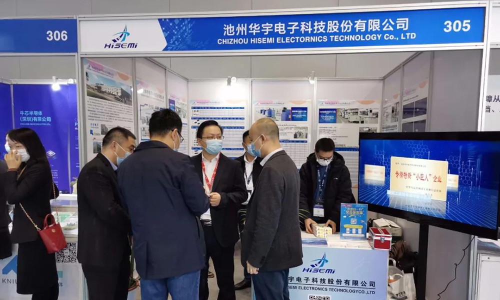
As a semiconductor packaging and testing enterprise, Hisemi Electronics provides one-stop solutions for customers. In the 2-day exhibition, the development momentum of the company in recent years was displayed to customers, suppliers and semiconductor industry personnel, from low PIN Count to high PIN Count, from traditional packaging to advanced packaging; Hisemi electronics is the first international first-class sealed test enterprise to forge ahead, attracted many customers and suppliers stop to discuss!

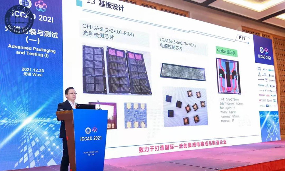
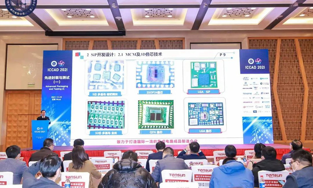
In the special forum on the second day, Mr Peng Yong, general manager of Hisemi Electronics, made a detailed discussion on “Hisemi Electronics explores SiP Integrated sealed test Solution”, and introduced huayu’s research and development capability, SiP development and design and SiP integrated sealed test solution to the industry colleagues attending in detail.
Chizhou Hisemi Electronic Technology Co., Ltd. was founded in 2006, and in 2013, mainly engaged in THE r&d of SOP/SOT/TO and other types of packaging test in the early stage. In 2018, it successfully developed and established the first QFN/DFN middle and high-end sealing test production line and framework SiP system level sealing test production line in Anhui Province. In 2020, the company’s strategic planning and R&D direction will move towards substrate SiP, such as LGA, BGA, FC, Bumping and WLCSP, mainly focusing on the relevant R&D and technological innovation in four areas including wafer testing, wafer thinning, IC packaging and IC finished product testing. Currently, WE are preparing LGA type SiP production line (including SMT), which is expected to be completed and put into operation in March 2022.


